I guess when you say EEPROM I think of the old black bug looking chips that you did have to have a charge pump circuit to erase and all that jazz for a chip that is only 8 bytes or something small like that. I have lots of equipment that still runs them and even some EPROM and PROM. Somewhere at work we have a UV lamp for erasing EPROMs.Flash is really "flash EEPROM", which is a type of EEPROM that is erased in entire blocks.
Flash memory is a type of electronically-erasable programmable read-only memory(EEPROM), but it can also be a standalone memory storage device such as a USB drive.
And absolutely blocks get erased. The idea is to get all the trapped charge in the "floating gate" out of there by zapping it. They have to be erased in order to program them, which involves injecting a precise amount of charge in the floating gate to change it's threshold voltage - the voltage that turns it on. I remember working with older flash where it was just one bit per transistor, and they could theoretically be written again without erasing. A block erase was always to all 1s. They could only be programmed to 0. So if a bit was still a 1, it could be programmed to 0, but if it was a 0 it could only stay at 0 until the block was erased. There were creative ways to use it where they didn't need to be erased.
As far as programming - that's pretty convoluted these days because single-level is no longer the standard except maybe for a high endurance cache. But the key is that it's not really programming the cell to sample an output like with SRAM or DRAM, but to program the threshold voltage that turns on a specific transistor. Then the voltage to turn on the transistor is tested. With single level, the goal is to program it for two different threshold voltages. With multi-level (2) it's four. With tri-level (3) it's eight. And with quad-level (4) it's sixteen. It's actually quite convoluted how this works and the more threshold voltages there might be programmed, the more complicated it is to test. When there are errors, there are different ways to adjust the thresholds to sample again. I don't fully understand all that stuff. I only understand this from a relatively high level. But there's less margin of error for more bits per cell.
There are all sorts of issues with accuracy as the insulator in a floating gate is damaged from erasing and programming. There's also the issue of charge in the floating gate leaking, which can be temperature dependent.
This shows the target threshold voltage for different cell capacities of flash.
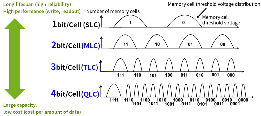
https://www.kioxia.com/en-jp/rd/technology/multi-level-cell.html
When I think flash memory it is surface mount components embedded on a board in something like a flash drive or other newer components. I believe the erasing progress is not as difficult as it used to be with the EEPROMs of old that had only one erase pin that cleared the whole chip. I am fairly sure that with modern SSDs like I said it is not physically erased off the chip till other data has been written into that block under normal circumstances to limit wear on the gates. This is why they tell you not to defrag an SSD because it just wears it out while not making anything faster because it is doing a lot of actual erasing.
 . The video I was watching about a voltage double was for serial coms. A charge pump is the same as a voltage doubler. Ben Eater on youtube has some great videos explaining stuff like this as he built an 8 bit computer on bread boards.
") All kidding aside they're wear items with a limited life cycle and planned obsolescence, so I plan accordingly.
All kidding aside they're wear items with a limited life cycle and planned obsolescence, so I plan accordingly.